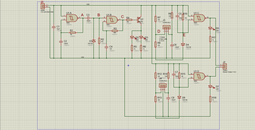
As a group of four, we all followed the module coordinator’s instructions closely to understand the process. Once we grasped the basic concept, each team member attempted to complete their own PCB design recreating the circuit on the right.
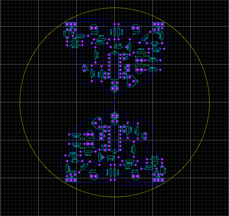
After reviewing everyone’s designs, only two of us were able to finalize a complete design. We discussed the options and agreed on the best design. The final design was then submitted to the module coordinator for approval.
A few days later, the printed PCB was prepared, and the necessary holes were ready for drilling. We carefully drilled the holes in the PCB according to the design specifications. With the holes drilled, we soldered the components onto the PCB, using the circuit diagram made in Proteus as our reference to ensure accuracy. After completing the soldering, the PCB assembly was finished and ready for the next stage of the project.
