Our PCB was constructed using a programme called Proteus, we used this particular programme as it was beginner friendly, it provided a wide range of features, and it had a good graphical interface. For instance, the programme allowed for hassle free placement of components and possessed the feature to model the PCB design in 3D, this would prove to be useful when soldering components onto the PCB.
For our PCB design we were provided with a pre-built circuit diagram, the circuit mainly consisted of the IR sensors and their circuitry. We used this diagram to assist us with the design and construction of the PCB. After we had placed and connected the components with bottom copper tracks, we added the components of our special feature into the existing circuit diagram. Afterwards, the additional components were placed onto the PCD alongside the IR circuitry. Finally, we had a finished PCB circuit that had both the IR circuitry and our special feature present. We decided to combine the two circuits onto one PCB in order to save materials and to reduce the overall profile of our Micromouse.
Before submitting our PCB design for approval and printing, we made sure to double and triple check that there were errors, these included that there were no missing components, no 90° turns in the tracks and that there were no Design Rule Check errors.
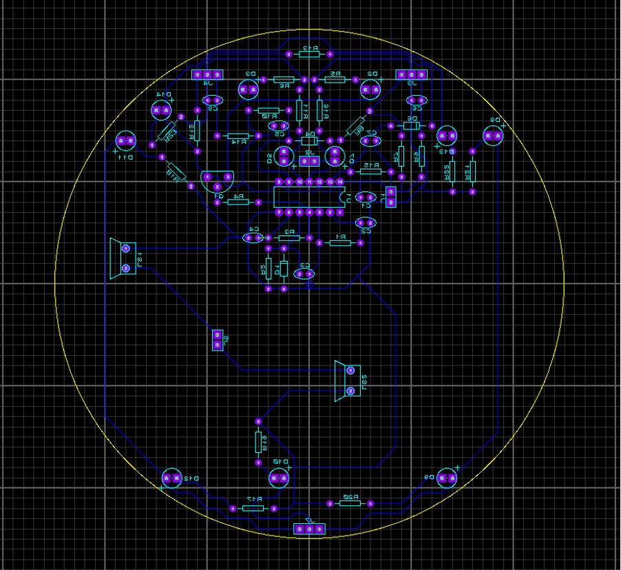
Picture of our PCB design constructed using Proteus, featuring the circuitry for the IR sensors and our special feature.
Once we received our grade for the PCB Design, we began to work on preparing the printed PCB for soldering. We first drilled the holes for the components, then we cut and sanded the PCB into the desired shape of a circuit. We then began the long process of soldering the components onto the copper tracks of the PCB.
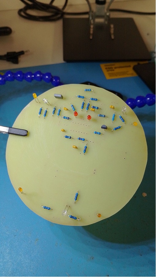
Picture of the printed PCB, in the process of having the components soldered onto it.
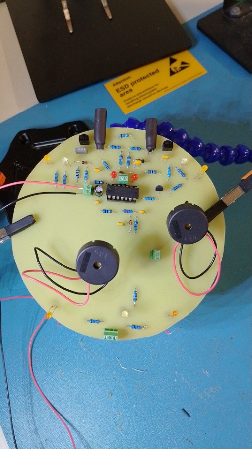
Picture of our fully complete PCB, featuring the components of the IR sensors and our special feature.