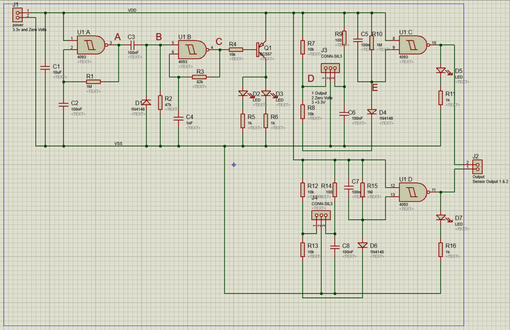
Schematic of PCB Design
Firstly, looking at the circuit diagram for the infra-red sensors and planning where abouts on the PCB all the components may want to go, ensuring that the sensors and receivers are located on the front.
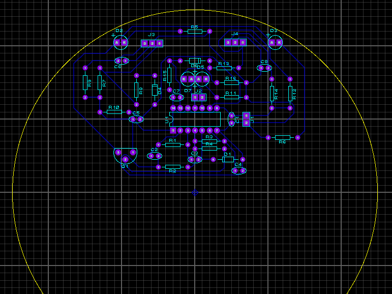
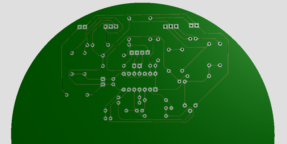
PCB Design on Proteus
Using Proteus alongside the circuit schematic to plan where all the components will go, trying to minimise the amount of space used to leave left over room in case we wish to add anything on the back of the PCB at a future date. Additionally ensuring that there are no right angles on the wiring which would cause issues in the future.
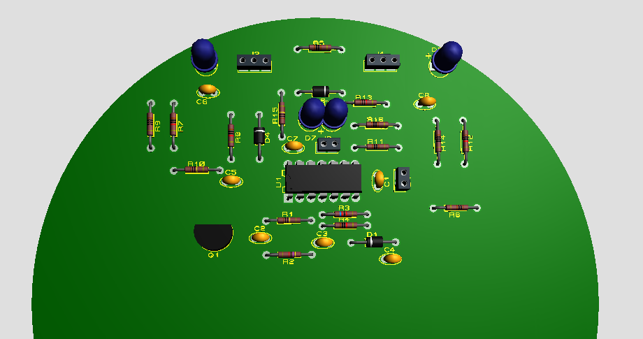
Preparing the PCB
Drilling holes where all the components needed to go trying to be as accurate as possible to make sure there are no issues with shorting and the PCB works as intended, then brushing down the top layer to expose the copper making it significantly easier to solder.
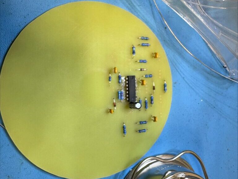
Soldiering the PCB
Soldiering all the components on to the PCB and transferring the calibrated infra-red sensors over to make sure everything is working properly as intended.